How Solar Works
Photovoltaics
Photovoltaic (PV) materials and devices convert sunlight into electrical energy, and PV cells are commonly known as Solar Cells. Photovoltaics can be translated as light electricity.
First used in about 1890, “photovoltaic” has two parts: photo, derived from the Greek word for light, and volt, relating to electricity pioneer Alessandro Volta. And this is what photovoltaic materials and devices do—they convert light energy into electrical energy, as French physicist Edmond Becquerel discovered as early as 1839.
Becquerel discovered using sunlight to produce an electric current in a solid material. But it took more than another century to understand this process truly. Scientists eventually learned that the photoelectric or photovoltaic effect caused certain materials to convert light energy into electrical energy at the atomic level.
Photovoltaic Cells
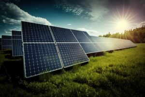
Photovoltaic (PV) or solar cells use the photoelectric effect to produce electricity. PV cells are the building blocks of all PV systems since they are the devices that convert sunlight to electricity.
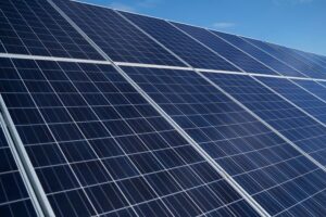
Commonly known as solar cells, individual PV cells are electricity-producing devices made of semiconductor materials. PV cells come in many sizes and shapes, from smaller than a postage stamp to several inches across. They are often connected from PV modules up to several feet long and a few feet wide.
Modules, in turn, can be combined and connected to form PV arrays of different sizes and power output. The array’s modules comprise the central part of a PV system, including electrical connections, mounting hardware, power-conditioning equipment, and batteries that store solar energy when the sun is not shining.
When light shines on a PV cell, it may be reflected, absorbed, or pass right through. But only the absorbed light generates electricity. The energy of the absorbed light is transferred to electrons in the atoms of the PV cell (see semiconductor material). With their newfound energy, these electrons escape from their regular positions in the atoms and become part of the electrical flow, or current, in an electrical circuit. A unique electrical property of the PV cell—called a “built-in electric field”—provides the force, or voltage, needed to drive the current through an external load, such as a light bulb.
Photovoltaic Systems
A photovoltaic (PV), or solar electric system, comprises several photovoltaic solar cells. An individual PV cell is usually small, producing about 1 or 2 watts of power. To boost the power output of PV cells, they are connected to form larger units called modules. Modules, in turn, can be connected to form even larger units called arrays, which can be interconnected to produce more power, and so on. This way, PV systems can be built to meet almost any electric power need, small or large.
The basic PV or solar cell produces only a tiny amount of power. Cells can be interconnected to form modules, which can be connected into arrays to produce more power. Because of this modularity, PV systems can be designed to meet any electrical requirement, whether large or small.
By themselves, modules or arrays do not represent an entire PV system. Systems also include structures that point them toward the sun and components that take the direct-current electricity produced by modules and “condition” that electricity, usually by converting it to alternate-current electricity. PV systems may also include batteries. These items are called the balance of system (BOS) components.
Combining modules with BOS components creates an entire PV system. This system is usually everything needed to meet a particular energy demand, such as powering a water pump, the appliances, and lights in a home, or—if the PV system is large enough—all the electrical requirements of a community.
Photovoltaic System Performance
Photovoltaic (PV) systems usually comprise multiple solar arrays comprising numerous PV cells. The system’s performance is, therefore, dependent on the performance of its components.
Reliability
The reliability of PV arrays is an essential factor in the cost of PV systems and consumer acceptance. However, the building blocks of arrays, PV cells, are considered “solid-state” devices with no moving parts and are highly reliable and long-lived. Therefore, reliability measurements of PV systems are usually focused not on cells but on modules and whole systems.
Reliability can be improved through fault-tolerant circuit design, which involves using various redundant features in the circuit to control the effect of partial failure on overall module yield and array power degradation. Degradation can be controlled by dividing the modules into several parallel solar cell networks called branch circuits. This type of design can also improve module losses caused by damaged cells and other circuit failures. Bypass diodes or other corrective measures can mitigate the effects of local cell hot spots. However, today’s component failure rates are low enough that, with multiple-cell interconnects, series/paralleling, and bypass diodes, it is possible to achieve high levels of reliability.
Module Performance Measurements
PV module performance is measured with peak watt ratings. The peak watt (Wp) rating is determined by measuring the maximum power of a PV module under laboratory conditions of relatively high light, good air mass, and low cell temperature. However, these conditions are not typical in the real world. Therefore, researchers may use a different procedure, known as the NOCT—or average operating cell temperature—rating. In this procedure, the module first equilibrates with a specified ambient temperature to measure maximum power at a nominal operating cell temperature. This NOCT rating results in a lower watt value than the peak-watt rating, but it is probably more realistic.
However, neither of these methods is designed to indicate the performance of a solar module under realistic operating conditions. Another technique, the AMPM Standard, involves considering the whole day rather than “peak” sunshine hours. This standard, intended to address the practical user’s needs, is based on the description of a standard solar global-average day (or a practical global average) in terms of light levels, ambient temperature, and air mass.
Solar arrays are designed to provide specified amounts of electricity under certain conditions. The following factors are usually considered when determining array performance: characterization of solar cell electrical performance, determination of degradation factors related to array design and assembly, conversion of environmental considerations into solar cell operating temperatures, and calculation of array power output capability.
Anyone, or a combination of the following performance criteria, may define the amount of electricity required:
• Power output
Power output is the power (in watts) available at the power regulator, specified as peak power or average power produced during one day.
• Energy output
The energy (watt-hour or Wh) output. This indicates the amount of energy produced during a specific period. The parameters are output per unit of array area (Wh/m2), output per unit of array mass (Wh/kg), and output per unit of array cost (Wh/$).
• Conversion efficiency
This parameter is defined as energy output from the array/energy input from sun x 100%. It is often given as power efficiency equal to the power output from the array/power input from the sun x 100%.
Power is typically given in units of watts (W), and energy is typically in watt-hours (W units).
Groups such as the Institute of Electrical and Electronics Engineers and the American Society for Testing and Materials are working on standards and performance criteria for PV systems to ensure the consistency and quality of photovoltaic systems and increase consumer confidence in system performance.
Semiconductors and the Built-In Electric Field for Crystalline Silicon Photovoltaic Cells
Crystalline silicon cells must have a built-in electric field to separate electrical charges. Light shining on crystalline silicon may free electrons within the crystal lattice, but for these electrons to do practical work—such as providing electricity to a light bulb—they must be separated and directed into an electrical circuit.
PV Semiconductors
Although both materials are electrically neutral, n-type silicon has excess electrons, and p-type silicon has excess holes. Sandwiching these together creates a p/n junction at their interface, creating an electric field.
Substituting a phosphorus atom (with five valence electrons) for a silicon atom in a silicon crystal leaves an extra, unbonded electron that is relatively free to move around the crystal.
Two silicon semiconductor layers are sandwiched to create an electric field within a crystalline silicon photovoltaic (PV) cell. P-type (or positive) semiconductors have an abundance of positively charged holes, and n-type (or unfavorable) semiconductors have an abundance of negatively charged electrons. When n- and p-type silicon layers contact, excess electrons move from the n-type side to the p-type side. The result is a buildup of positive charge along the n-type side of the interface and a buildup of negative charge along the p-type side.
The two semiconductors behave like a battery because of the flow of electrons and holes, creating an electric field at the surface where they meet. This area where they meet is called the p/n junction. The electrical field causes the electrons to move from the semiconductor toward the opposing surface, making them available for the electrical circuit. At the same time, the holes move in the opposite direction toward the positive surface, where they await incoming electrons.
Power Inverter
Power conditioners process the electricity produced by a PV system so it will meet the specific demands of the load. Although most equipment is standard, it is crucial to select equipment that matches the characteristics of the load. Power conditioners may:
• Limit current and voltage to maximize power output
• Convert DC power to AC power
• Match the converted AC electricity to a utility’s electrical network
• Have safeguards that protect utility personnel and the electrical network from harm during repairs.
Specific requirements of power conditioners depend on the type of PV system they are used with and the applications of that system. For DC applications, power conditioning is often done with regulators, which control output at some constant level of voltage and current to maximize output. For AC loads, power conditioning must include an inverter that converts the DC power generated by the PV array into AC power. Many simple devices—for example, ones that run on batteries—use DC electricity. However, AC electricity, which is what is generated by utilities, is needed to run most modern appliances and electronic devices.
Mounting Structures
PV arrays must be mounted on a stable, durable structure that can support the array and withstand wind, rain, hail, and other adverse conditions. Sometimes, this mounting structure is designed to track the sun. However, stationary structures are usually used with flat-plate systems. These structures tilt the PV array at a fixed angle determined by the site’s latitude, load requirements, and sunlight availability.
Rack mounting may be the most versatile choice for stationary mounting structures. It can be constructed relatively quickly and installed on the ground or flat or slanted roofs.
There are two basic kinds of tracking structures: one-axis and two-axis. One-axis trackers are typically designed to track the sun from east to west. They are used with flat-plate systems and sometimes with concentrator systems. The two-axis type is used primarily with PV concentrator systems. These units track the sun’s daily and seasonal course between the northern and southern hemispheres. Naturally, the more sophisticated systems are more expensive and require more maintenance.
Crystalline Silicon Photovoltaic Cells
Crystalline silicon cells are made of silicon atoms connected to form a crystal lattice. This lattice comprises the solid material that forms the photovoltaic (PV) cell’s semiconductors. This section describes the atomic structure and bandgap energy of these cells.
Atomic Structure
All matter comprises atoms comprising positively charged protons, negatively charged electrons, and neutral neutrons. Protons and neutrons, which are about the same size, are in the close-packed, central nucleus of the atom. The much lighter electrons orbit the nucleus. Although atoms are built of oppositely charged particles, their overall charge is neutral because they contain an equal number of positive protons and negative electrons, whose charges offset each other.
As depicted in this simplified diagram, silicon has 14 electrons. The four electrons that orbit the nucleus in the outermost “valence” energy level are given to, accepted from, or shared with other atoms.
In the basic unit of a crystalline silicon solid, a silicon atom shares its four valence electrons with each of the four neighboring atoms.
Electrons orbit at different distances from the nucleus, depending on their energy level—electrons with less energy orbit close to the nucleus, and electrons with more energy orbit farther away. The higher-energy electrons farthest from the nucleus are the ones that interact with neighboring atoms to form solid structures.
A silicon atom has 14 electrons, but their natural orbital arrangement allows only the outermost four electrons to be given to, accepted from, or shared with other atoms. These four electrons, called valence electrons, are essential in the photoelectric effect.
Many silicon atoms bond with one another using their valence electrons to form a crystal. In a crystalline solid, each silicon atom typically shares one of its four valence electrons in a covalent bond with four neighboring silicon atoms. The solid thus consists of basic units of five silicon atoms: the original atom plus the four atoms with which it shares valence electrons.
The solid silicon crystal is thus made up of a regular series of units of five silicon atoms. This regular, fixed arrangement of silicon atoms is known as the crystal lattice.
Creating P-Type and N-Type Semiconductors
In a crystalline silicon PV cell, p-type silicon must contact n-type silicon to create the built-in electrical field. Doping, which is used to create these materials, introduces an atom of another element into silicon crystal to alter its electrical properties. The dopant, the introduced element, has three or five valence electrons—one less or more than silicon’s four.
Phosphorus atoms with five valence electrons are used to dope n-type silicon because phosphorus provides its fifth free electron. A phosphorus atom occupies the same place in the crystal lattice formerly occupied by the silicon atom it replaced. Four of its valence electrons take over the bonding responsibilities of the four silicon valence electrons that they replaced. But the fifth valence electron remains free, having no bonding responsibilities. When phosphorus atoms are substituted for silicon in a crystal, many free electrons become available.
The most common doping method is to coat a layer of silicon material with phosphorus and then heat the surface. This allows the phosphorus atoms to diffuse into the silicon. The temperature is then reduced, so the diffusion rate drops to zero. Other methods of introducing phosphorus into silicon include gaseous diffusion, a liquid dopant spray-on process, and a technique in which phosphorus ions are precisely driven into the surface of the silicon.
However, the n-type silicon cannot form an electric field by itself. It also needs p-type silicon. Boron, which has only three valence electrons, is used for doping p-type silicon. Boron is introduced during silicon processing when the silicon is purified for use in photovoltaic devices. When a boron atom takes a position in the crystal lattice formerly occupied by a silicon atom, a bond will miss an electron. In other words, there is an extra positively charged hole.
P-Layer Design
In a PV cell, photons are absorbed in the player. Therefore, this layer must be “tuned” to the properties of incoming photons so it can absorb as many as possible and, thus, free up as many electrons as possible. The player’s design must also keep the electrons from meeting up with holes and recombining with them before they can escape from the PV cell. To accomplish these goals, players are designed to free electrons as close to the junction as possible so that the electric field can help send the free electrons through the conduction layer (the n-layer) and out into the electrical circuit.
By optimizing these characteristics, the PV cell’s conversion efficiency (how much light energy is converted into electrical energy) is improved.
Bandgap Energy
Bandgap energy is required to dislodge an electron from its covalent bond and allow it to become part of an electrical circuit. When light shines on crystalline silicon, electrons within its crystal lattice may be freed. But not all photons—as packets of light energy are called—are created equal.
To free an electron, the energy of a photon must be at least as great as the bandgap energy. However, photons with more energy than the bandgap energy will expend the extra heat when freeing electrons. So, a photovoltaic (PV) cell must be “tuned”—through slight modifications to the silicon’s molecular structure—to optimize the photon energy.
Crystalline silicon has a bandgap energy of 1.1 electron volts (eV). (An electron volt is equal to the energy gained by an electron when it passes through a potential of 1 volt in a vacuum.) The bandgap energies of other effective PV semiconductors range from 1.0 to 1.6 eV. In this range, electrons can be freed without creating extra heat.
The photon energy of light varies according to the wavelengths of the light. The entire spectrum of sunlight, from infrared to ultraviolet, covers a range of about 0.5 eV to about 2.9 eV. For example, red light has an energy of about 1.7 eV, and blue light has an energy of about 2.7 eV. Most PV cells cannot use about 55% of the energy of sunlight because this energy is either below the bandgap of the material used or carries excess energy.
Different PV materials have different energy band gaps. Photons with energy equal to the band gap energy are absorbed to create free electrons. Photons with less energy than the band gap energy pass through the material.